- Published on
A computer that runs on light, not electricity? It sounds like sci-fi, but the chip already works
- Authors

- Name
- aimode.news
- @aimode_news
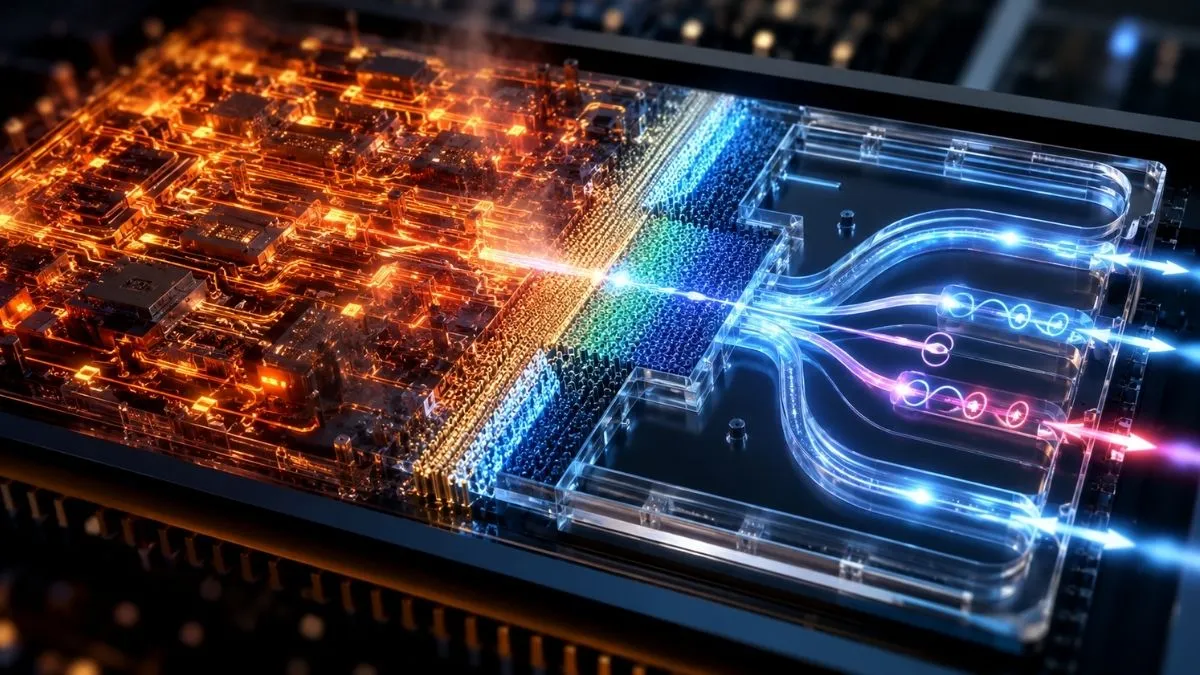
Computers don't slow down because electrons suddenly stop working. The problem is that transmitting data through electricity increasingly means heat, delays and huge energy consumption. That's why scientists are trying to move some of the computation and communication to the world of light. A team from Monash University has just shown a chip that can generate, conduct and read information carried by photons in one place.
The chip doesn't throw away electrons, but it gives light a bigger role
The new chip is not a classic processor that will replace CPU or GPU in your computer. We are talking about an optoelectronic nanochip, i.e. one that combines light and electronics in one system.
The biggest breakthrough is the integration of three things that were previously difficult to combine in one compact structure. The chip can produce special light signals, direct them along specific paths, and convert the final signal into an electrical readout. It is of great importance for integrated photonics. Merely generating a signal is not enough if it cannot be routed. Merely guiding the light is not enough if it cannot be read precisely.
This arrangement is therefore more of a demonstration of a complete information chain than of a single physical effect. The light here is not a decoration or a carrier in an optical cable away from the chip. It becomes part of the information processing itself on the surface of the system.
The current begins to lose its own success
Modern computers are truly impressive, but their fundamental problem is becoming increasingly physical. Electrons sent through metal paths do not move for free. The more data that needs to be moved between processors, memory, AI accelerators and the network, the more energy turns into heat. In data centers, this is one of the main operating costs.
Artificial intelligence exacerbates this problem even further. AI models not only perform calculations, but also constantly crunch gigantic amounts of data. Increasingly, the limitation is not the counting itself, for which computers were designed, but the communication between system elements. Data has to get to where it is needed, and each move costs energy and time.
Light has some very big advantages here. First of all, it can transfer huge amounts of information, it does it extremely quickly and does not generate the same losses as transmitting electrical signals over increasingly greater distances inside systems. That's why we've been using them in fiber optics for a long time. Now researchers are trying to introduce optical elements directly into the chips, so that data does not have to be transported solely by electrons all the time.
Atomically thin materials do the most work here
Monash University's system uses materials so thin that their thickness is measured in single atomic layers. The work includes, among others: tungsten disulfide and tungsten diselenide, belonging to the group of transition metal dichalcogenides. These are materials that have been of great interest to physicists for years, because on a 2D scale they can have properties completely different from those of classic semiconductors.
Tungsten disulfide can generate valley-dependent photons when excited with carefully selected light. In turn, several layers of tungsten diselenide were used as photodetectors that read the signal. A nanostructure works between them, guiding light in a specific direction.
So it is a well-thought-out sandwich with several elements. An atomically thin layer generates a signal, a special metasurface and waveguide direct it further, and another ultrathin material turns it into an electrical readout.
This is where another important element of the system comes into play: the metasurface. Between the signal generating layer and the detector there is a nanostructure responsible for directing the light. This is the metasurface, i.e. an artificially designed surface covered with very small structures that allow precise control of the behavior of photons. Thanks to it, the signal can be directed to the appropriate waveguide channel instead of spreading randomly.
The chip guides the light in one direction
One of the most important results is the selective guidance of chiral photons. Chirality means that an object or phenomenon has rotation, just as the right and left hands are reflections of each other, but they cannot be perfectly superimposed. In optics, chirality can be related to the circular polarization of light.
In the new arrangement, valley-dependent signals can be directed to specific sides of the waveguide. A waveguide is the equivalent of a wire for light. Instead of carrying electrons, it carries photons. If a chip can make a certain signal go one way and another signal go the other way, it starts to look like a miniature information sorting system.
The publication provides a very high polarization selectivity, reaching 0.97. This means that the system is very effective at distinguishing and transmitting the right signals. This is an important parameter for the laboratory, because it shows that it is not about a barely noticeable effect, but about control at a level that may make sense in further device design.
It is this element that brings the whole thing closer to the creation of practical systems. Information must not only be created, but also sent to the right place without mixing channels.
The biggest obstacles are production and scale
As is usually the case with such discoveries, you have to separate the beauty of the experiment from the real industry. The system works, but the road to mass production is long. Atomically thin materials must be produced reproducibly, precisely arranged on photonic structures, integrated into existing chip production processes, and ensured stable operation over the long term.
An important element here is the layering itself. The researchers emphasize that they used a relatively simple method of applying ultrathin materials to metasurfaces, bypassing the problem of direct material growth on complex photonic structures. This may facilitate further work, but does not mean that the technology is ready for production in semiconductor factories.
Read also:
The chip industry doesn't love solutions that only work in a single sample. It needs hundreds, thousands and millions of repeating patterns. Must know tolerances, durability, performance, cost, and compatibility with the rest of the electronics. Only then can we talk about technology that will go beyond scientific publications.
*Introductory graphics generated by AI